- 您现在的位置:买卖IC网 > Sheet目录17338 > ISL8201MEVAL1Z (Intersil)BOARD EVAL STEP-DOWN POL ISL8201
�� �
�
�ISL8201M�
�Pin� Functions�
�PGND� (Pins� 1,� 2,� 3,� 4,� 11)�
�Power� ground� pin� for� signal,� input,� and� output� return� path.�
�PGND� needs� to� connect� to� one� (or� more)� ground� plane(s)�
�immediately,� which� is� recommended� to� minimize� the� effect� of�
�switching� noise,� copper� losses,� and� maximize� heat� dissipation.�
�PVCC� (Pin� 5)�
�This� pin� provides� the� bias� supply� for� ISL8201M,� as� well� as�
�the� low-side� MOSFET’s� gate� and� high-side� MOSFET’s� gate.�
�If� PVCC� rises� above� 6.5V,� an� internal� 5V� regulator� will�
�supply� to� the� internal� logics� bias� (but� high-side� and� low-side�
�MOSFET� gate� will� still� be� sourced� by� PVCC).� Connect� a� well�
�decoupled� +5V� or� +12V� supply� to� this� pin.�
�NC� (Pins� 6,� 8,� 15)�
�These� pins� have� no� function;� do� not� connect.�
�ISET� (Pin� 7)�
�The� ISET� pin� is� the� input� for� the� overcurrent� protection�
�(OCP)� setting,� which� compares� the� r� DS(ON)� of� the� low-side�
�MOSFET� to� set� the� overcurrent� threshold.� The� ISL8201M�
�has� an� initial� protect� overcurrent� limit.� It� has� an� integrated�
�internal� 3.57k� Ω� resistor� (R� SET-IN� )� between� the� ISET� and�
�PGND� pins,� which� can� prevent� significant� overcurrent� impact�
�to� the� module.� One� can� also� connect� an� additional� resistor�
�high-side� gate� and� low-side� gate� of� the� MOSFETs� outputs� to�
�be� held� low.� The� external� pull-down� device� will� initially� need�
�to� overcome� a� maximum� of� 5mA� of� COMP/EN� output�
�current.� However,� once� the� controller� is� disabled,� the�
�COMP/EN� output� will� also� be� disabled,� thus� only� a� 20μA�
�current� source� will� continue� to� draw� current.�
�FB� (Pin� 14)�
�The� FB� pin� is� the� output� voltage� adjustment� of� the� ISL8201M.�
�It� will� regulate� to� 0.6V� at� the� FB� pin� with� respect� to� the� PGND�
�pin.� The� ISL8201M� has� an� integrated� voltage� dividing� resistor.�
�This� is� a� precision� 9.76k� Ω� resistor� (R� FB-TI� )� between� the� VOUT�
�and� FB� pins.� Different� output� voltages� can� be� programmed�
�with� additional� resistors� between� FB� to� PGND.�
�Reference� Circuitry� For� General�
�Applications�
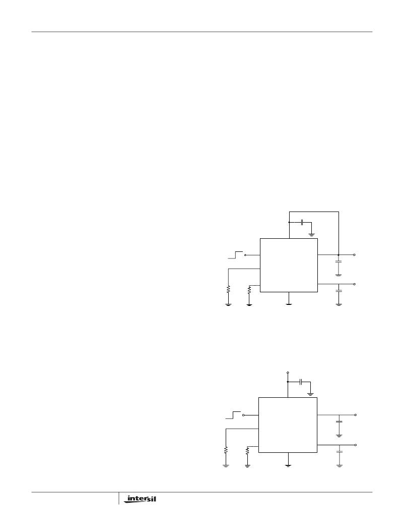
�Typical� Application� with� Single� Power� Supply�
�Figure� 11� shows� the� ISL8201M� application� schematic� for�
�input� voltage� +5V� or� +12V.� The� PVCC� pin� can� connect� to� the�
�input� supply� directly.�
�C� PVCC�
�PVCC�
�R� SET-EX� between� the� ISET� pin� and� the� PGND� pin� in� order� to�
�reduce� the� current� limit� point� by� paralleling.�
�COMP/EN�
�ISL8201M�
�VIN�
�(+5V/+12V)�
�V� IN�
�C� IN�
�VIN� (Pin� 9)�
�Power� input� pin.� Apply� input� voltage� between� the� VIN� pin�
�FB�
�PHASE�
�V� OUT�
�and� PGND� pin.� It� is� recommended� to� place� an� input�
�decoupling� capacitor� directly� between� the� VIN� pin� and� the�
�R� FB�
�R� SET-EX�
�ISET�
�PGND�
�VOUT�
�C� OUT�
�PGND� pin.� The� input� capacitor� should� be� placed� as� closely�
�as� possible� to� the� module.�
�PHASE� (Pin� 10)�
�The� PHASE� pin� is� the� switching� node� between� the� high� and�
�low� side� MOSFET.� It� also� returns� the� current� path� for� the�
�high� side� MOSFET� driver� and� detects� the� low-side� MOSFET�
�drain� voltage� for� the� overcurrent� limits� point.�
�FIGURE� 11.� TYPICAL� APPLICATION� SCHEMATIC�
�Typical� Application� with� Separated� Power� Supply�
�Figure� 12� shows� the� ISL8201M� application� schematic� for�
�wide� input� voltages� from� +1V� to� +20V.� The� P� VCC� supply� can�
�source� +5V/+12V� or� +6.5V� to� 14.4V.�
�VOUT� (Pin� 12)�
�(+5V/+12V)�
�or�
�P� VCC�
�Power� output� pin.� Apply� output� load� between� this� pin� and� the�
�PGND� pin.� It� is� recommended� to� place� a� high� frequency�
�output� decoupling� capacitor� directly� between� the� VOUT� pin�
�(+6.5V� to� 14.4V)�
�C� PVCC�
�and� the� PGND� pin.� The� output� capacitor� should� be� placed� as�
�PVCC�
�closely� as� possible� to� the� module.�
�COMP/EN� (Pin� 13)�
�COMP/EN�
�ISL8201M�
�VIN�
�(+1V� to� +20V)�
�C� IN�
�V� IN�
�This� is� the� multiplexed� pin� of� the� ISL8201M.� During� soft-start�
�and� normal� converter� operation,� this� pin� represents� the�
�FB�
�PHASE�
�V� OUT�
�output� of� the� error� amplifier.� Use� COMP/EN� in� combination�
�with� the� FB� pin� to� compensate� for� the� voltage� control�
�R� FB�
�R� SET-EX�
�ISET�
�PGND�
�VOUT�
�C� OUT�
�feedback� loop� of� the� converter.� Pulling� COMP/EN� low�
�(V� ENDIS� =� 0.4V� nominal)� will� disable� (shut-down)� the�
�controller,� which� causes� the� oscillator� to� stop,� and� the�
�7�
�FIGURE� 12.� WIDE� INPUT� VOLTAGE� APPLICATION� SCHEMATIC�
�FN6657.2�
�October� 21,� 2010�
�发布紧急采购,3分钟左右您将得到回复。
相关PDF资料
EEC15DREI-S13
CONN EDGECARD 30POS .100 EXTEND
RCM15DCSH-S288
CONN EDGECARD 30POS .156 EXTEND
EEC20DREH-S13
CONN EDGECARD 40POS .100 EXTEND
RCC07DRXI
CONN EDGECARD 14POS DIP .100 SLD
594D106X9020B8T
CAP TANT 10UF 20V 10% 1611
TARS226M010
CAP TANT 22UF 10V 20% AXIAL
EBC15DCMI
CONN EDGECARD 30POS .100 WW
A9BAG-1606F
FLEX CABLE - AFF16G/AF16/AFE16T
相关代理商/技术参数
ISL8201MIRZ
功能描述:DC/DC转换器 STAND ALONE 10A DC/D CSTEPDWNPWRSUPPYMOD1
RoHS:否 制造商:Murata 产品: 输出功率: 输入电压范围:3.6 V to 5.5 V 输入电压(标称): 输出端数量:1 输出电压(通道 1):3.3 V 输出电流(通道 1):600 mA 输出电压(通道 2): 输出电流(通道 2): 安装风格:SMD/SMT 封装 / 箱体尺寸:
ISL8201MIRZ-T
功能描述:DC/DC转换器 ST& ALONE 10A DC/DC DWN PWR SUPPLY MOD RoHS:否 制造商:Murata 产品: 输出功率: 输入电压范围:3.6 V to 5.5 V 输入电压(标称): 输出端数量:1 输出电压(通道 1):3.3 V 输出电流(通道 1):600 mA 输出电压(通道 2): 输出电流(通道 2): 安装风格:SMD/SMT 封装 / 箱体尺寸:
ISL8204M
制造商:INTERSIL 制造商全称:Intersil Corporation 功能描述:Complete High Efficiency DC/DC Power Module
ISL8204MEVAL1Z
功能描述:电源管理IC开发工具 ISL8204 EVAL BRD 1 ROHS CMPL MOD
RoHS:否 制造商:Maxim Integrated 产品:Evaluation Kits 类型:Battery Management 工具用于评估:MAX17710GB 输入电压: 输出电压:1.8 V
ISL8204MIRZ
功能描述:DC/DC转换器 STAND ALONE 4A DC/DC STEPDWNPWRSUPPYMOD15
RoHS:否 制造商:Murata 产品: 输出功率: 输入电压范围:3.6 V to 5.5 V 输入电压(标称): 输出端数量:1 输出电压(通道 1):3.3 V 输出电流(通道 1):600 mA 输出电压(通道 2): 输出电流(通道 2): 安装风格:SMD/SMT 封装 / 箱体尺寸:
ISL8204MIRZ-T
功能描述:DC/DC转换器 ST& ALONE 4A DC/DC DWN PWR SUPPLY MOD RoHS:否 制造商:Murata 产品: 输出功率: 输入电压范围:3.6 V to 5.5 V 输入电压(标称): 输出端数量:1 输出电压(通道 1):3.3 V 输出电流(通道 1):600 mA 输出电压(通道 2): 输出电流(通道 2): 安装风格:SMD/SMT 封装 / 箱体尺寸:
ISL8206M
制造商:INTERSIL 制造商全称:Intersil Corporation 功能描述:Complete High Efficiency DC/DC Power Module
ISL8206MEVAL1Z
功能描述:电源管理IC开发工具 ISL8206 EVAL BRD 1 ROHS CMPL MOD
RoHS:否 制造商:Maxim Integrated 产品:Evaluation Kits 类型:Battery Management 工具用于评估:MAX17710GB 输入电压: 输出电压:1.8 V